mww2
mww2
8 Best PCB Design Software for Every Skill Level
Designing printed circuit boards (PCBs) isn’t just about connecting lines and placing components. It’s about choosing the right tool that does what you need without making things harder than they should be. Whether you’re just starting out or have years of experience, the software you use can make a big difference in how efficient, accurate, and headache-free your workflow feels. Here are some of the best PCB design tools available right now.
What Are the Best Software for Making PCBs?
KiCad
KiCad is a free, open-source PCB design tool that doesn’t feel like a compromise. You get features like 3D visualization, a built-in SPICE simulator, and a helpful footprint editor. It supports multi-sheet schematics and unlimited board sizes, which isn’t something all free tools offer. What makes KiCad stand out is the community—users are quick to share libraries, footprints, and even full design templates. It’s a solid pick for those who want control and flexibility without opening their wallet.
Altium Designer
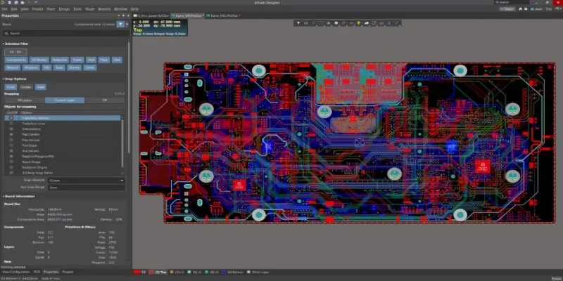
Altium Designer is the go-to for engineers who need a serious tool with a lot under the hood. It comes with advanced routing options, a unified interface for schematic and PCB layout, and solid support for rigid-flex designs. Collaboration tools are baked in, so you can share designs with team members and manufacturers in real-time. It isn’t cheap, but its polish and depth of features keep it at the top of the food chain for professionals who can justify the cost.
EasyEDA
If browser-based tools appeal to you, EasyEDA is worth a look. It runs entirely online, so you don’t need to download anything. This makes it especially appealing to hobbyists or anyone using a less powerful computer. You can import files, simulate circuits, and even order boards directly through the platform. For people new to PCB design, the interface feels simple enough to learn quickly but still covers a lot of ground as you grow more confident.
EAGLE (by Autodesk)
EAGLE has been around for a while and has a reputation for being beginner- friendly. Now, under Autodesk, it’s integrated with Fusion 360, which is great if you’re into mechanical design too. EAGLE lets you design schematics, create board layouts, and even run electrical rule checks. It also includes a robust library of parts, which cuts down the time spent searching or building components from scratch. While the free version is a bit limited, the paid options open things up considerably.
DipTrace
DipTrace is often chosen for its clean interface and smooth workflow. It includes tools for schematic capture, PCB layout, component creation, and even signal integrity verification. The learning curve is a bit flatter here compared to some others, which makes it appealing for small businesses or solo designers who want something intuitive. It also supports importing and exporting formats from other design tools, making it easier to switch or collaborate.
DesignSpark PCB

DesignSpark PCB is another free option, but it doesn’t feel half-baked. It provides schematic capture, PCB layout, and even 3D visualization. One of its standout features is unlimited board size, which isn’t common in free software. It’s ideal for students or budget-conscious professionals who still want access to advanced features. Plus, being tied to RS Components means easy access to a wide range of parts and data sheets.
OrCAD
OrCAD leans into the enterprise world with a heavy focus on simulation and signal integrity. It’s packed with tools that help you catch errors before they happen, like detailed electrical rule checks and thermal simulation. OrCAD is especially popular in industries where reliability isn’t optional, such as automotive or aerospace. It’s not the easiest tool to pick up if you’re new to PCB design, but it’s one of the most trusted once you get the hang of it.
Fritzing
Fritzing isn’t trying to compete with the big names—it’s meant to be beginner- friendly and visual. Designed for makers, educators, and hobbyists, it lets you go from breadboard to schematic to PCB with minimal confusion. The drag- and-drop interface is ideal for people who are more comfortable thinking visually. While it doesn’t offer the depth of tools like Altium or OrCAD, it’s a fun way to bring simple projects to life quickly.
How to Use Software for Making PCBs?
Among all the tools listed above, KiCad stands out for hitting the sweet spot between functionality and accessibility. In this section, we’ll go through how to actually use it—from the first click to generating files for manufacturing.
Once you launch KiCad, you’ll find yourself on a project manager screen. Start by creating a new project and naming it. Then, head into the schematic editor. Here, you can drag in components using the ‘Place Symbol’ tool. Search by part name or browse categories until you find what you need. After placing your parts, use the wire tool to make connections. Make sure each wire connects properly—hover over pins until they snap into place.
When your schematic is done, hit the “Assign Footprints” tool. This matches each symbol in your schematic with the actual physical footprint it will use on the PCB. After confirming the assignments, move into the PCB layout editor. Click “Update PCB from Schematic” to bring in the parts, and they’ll appear bunched together. Now, arrange the components manually. Use the ‘Route Tracks’ tool to lay down your traces. Keep an eye on clearances and try to avoid 90-degree corners where possible.
Once you’re happy with your layout, run the DRC (Design Rule Check) to catch issues. Then, generate Gerber files using the “Plot” tool. You’ll send these files to a PCB manufacturer. Don’t forget to generate a drill file as well. Save everything in a folder, zip it up, and you’re ready to order your board.
Final Thoughts
Choosing PCB design software isn’t about finding the “best” one overall—it’s about finding the one that fits how you work. Some tools are built for precision engineering, others for quick experiments or visual learners. KiCad, with its balance of depth and ease, often becomes the go-to for many designers across skill levels. Whatever your project looks like, using the right tool will make the process smoother, the outcome better, and the experience far less frustrating.
Related Articles

Top Online Graphic Design Tools for 2025: Canva, Figma, and More
Top Online Graphic Design Tools for 2025: Canva, Figma, and More

7 Smart Ways Adobe Express AI Can Instantly Boost Your Design Productivity

Discover the 9 Best Tools for Modern Web Design in 2025

The 8 Best To-Do List Apps for Android in 2025

Top Movie Making Tools for New Creators and Experienced Editors

Best Free Alternatives to Adobe for Creatives and Professionals

The 6 Best Construction Management Software Options to Streamline Your Projects

Top 7 UI/UX Design Tools Every Designer Should Know

The Best Employee Onboarding Software: Transforming New Hire Experiences

CapCut, WeVideo & More: Tools That Simplify Video Editing

10 Best Meeting Scheduler Apps to Try in 2025
Popular Articles

Experience AI Video Upscaling with Topaz in Freepik AI Suite Now

Explore the 10 Best Video Editing Software for Creators

Best Camcorders of 2025: Create Stunning Home Videos with Ease

AVCLabs Video Enhancer AI: Is It Really Worth Your Trial?

Simple Ways to Transfer Files Between Phone and PC

Slack vs. Teams: Which Should Your Business Use for Better Collaboration

Smartsheet vs. Asana: Which Project Management App is Right for You?
The 6 Best Squarespace Alternatives in 2025 for Custom, Creative Web Design

Stop Motion Made Easy with Windows Movie Maker: A Complete Tutorial

How Can You Supercharge Your Webinar Marketing with WebinarGeek?
The Easiest Way to Make Any Video Work with iTunes